Description
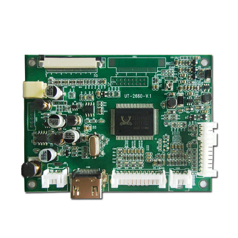
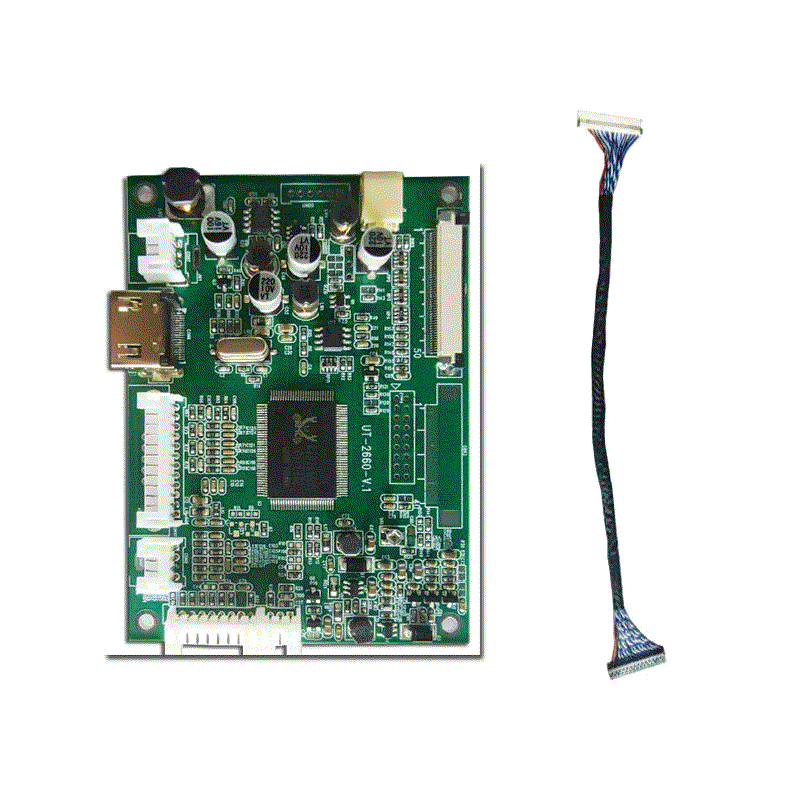
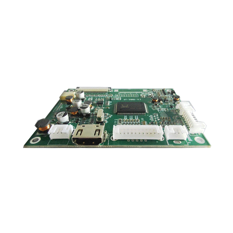
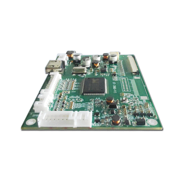
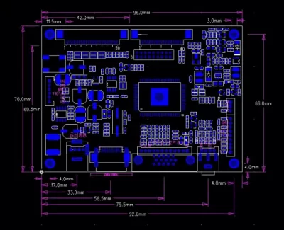
UT-2660V.1 TFT Driver Board
The RGB interface in the UT-2660V.1 TFT Driver Board has distinct advantages. It shows high compatibility with various small to medium-sized display panels. With a bandwidth of 1.2GB per second, it enables efficient high-res image data transmission. Also, it allows the MCU to directly update the screen for easy control.
The TFT technology in this driver board offers great benefits. It provides excellent image quality with independent pixel control and high brightness, contrast, etc. It's power-efficient, extending portable device battery life. Its lightweight and thin design saves space and suits mobile devices. It has a long lifespan, stable performance, and is eco-friendly and harmless to users.
Scope of Application:
TTL: Applicable to the inspection of driver boards for liquid crystal display modules such as EJ050NA - 01G, AT070TN92, AT070TN94, AT080TN64, AT080TN52, EJ080NA - 05A, EJ080NA - 05B, TM080RDH01, and AT090TN12.
LVDS: Applicable to the inspection of high - definition 40PIN liquid crystal display module driver boards such as EJ070NA - 01J, N070LGE - L41, HJ070NA - 13A, HJ070NA - 13B, EJ070NA - 01F, ZJ070NA - 01P, NJ070NA - 23A, P070BAG - CM1, TM070JDHG30, EJ080NA - 04C, HE080IA - 01D, HJ080NA - 04L, HJ080IA - 01F, TM080TDH01, and TM080TDHG01.
✅Product Function Description
1 Supports HDMI, VGA, and CVBS video signal input.
2 The power input is DC +12V.
3 Features multi - function OSD operation.
4 Optional remote control function is available.
5 Auto - power - off when no signal is detected.
✅ Signal Input Standards
1 HDMI: (Universal version 1.2).
2 VGA: Supports resolutions of 800×480, 800×600, 1024×600, 1024×768, 1280×800 (refresh rate 60 - 75Hz).
3 CVBS: 1.0Vp - p 75Ω. |
 |
| Interface Definition |
| CON3 (FPC Socket Definition) 40PIN/0.5MM |
| Pin No. |
Function |
Pin No. |
Function |
Pin No. |
Function |
Pin No. |
Function |
| 1 |
LED+ |
11 |
HS |
21 |
G6 |
31 |
R4 |
| 2 |
LED+ |
12 |
B7 |
22 |
G5 |
32 |
R3 |
| 3 |
LED- |
13 |
B6 |
23 |
G4 |
33 |
R2 |
| 4 |
LED- |
14 |
B5 |
24 |
G3 |
34 |
R1 |
| 5 |
GND |
15 |
B4 |
25 |
G2 |
35 |
R0 |
| 6 |
VCOM |
16 |
B3 |
26 |
G1 |
36 |
GND |
| 7 |
VCC |
17 |
B2 |
27 |
G0 |
37 |
DCLK |
| 8 |
MODE |
18 |
B1 |
28 |
R7 |
38 |
GND |
| 9 |
DE |
19 |
B0 |
29 |
R6 |
39 |
L/R |
| 10 |
VS |
20 |
G7 |
30 |
R5 |
40 |
U/D |
| CON6 (HDMI Input) Interface |
| Pin No. |
Function |
|
Pin No. |
Function |
|
|
|
| 1 |
TMDS Data 2+ |
|
11 |
TMDS Clock Shield |
|
|
|
| 2 |
TMDS Data Shield |
|
12 |
TMDS Clock - |
|
|
|
| 3 |
TMDS Data 2- |
|
13 |
CEC |
|
|
|
| 4 |
TMDS Data 1+ |
|
14 |
NC |
|
|
|
| 5 |
TMDS Data Shield |
|
15 |
SCL |
|
|
|
| 6 |
TMDS Data 1- |
|
16 |
SDL |
|
|
|
| 7 |
TMDS Data 0+ |
|
17 |
DDC/CEC GND |
|
|
|
| 8 |
TMDS Data Shield |
|
18 |
+5V |
|
|
|
| 9 |
TMDS Data 0- |
|
19 |
Hot Plug Detect |
|
|
|
| 10 |
TMDS Clock+ |
|
|
|
|
|
|